一所懸命HWデザイナーのふりをやっとる現代のC++が大嫌いなSWの開発者。FPGAのGPUとレトロな家庭用ゲーム機を作ること、うちの猫(ニュートリノ+コスモス)、お箏の演奏、ゲーム開発、抹茶+和菓子がめっさ好きやねん。tweetsは私個人の意見で、会社を代表するものやない
The Introduction
Self-review time at work always makes me depressed. Something about me is just fundamentally incompatible with writing long paragraphs about how amazing and indispensable I am, and without my primary weapon of self-deprecation, I am left essentially defenceless. And so to cheer myself up, I am doing a short post on one of my favourite topics: evaluating memory systems! Plus with the new rasterizer block done, and with texturing and primitive construction on the horizon, its starting to get a little late to begin to understand the capabilities of the Zynq memory system
Small disclaimer: to save time, I am going to assume you guys all know how RAM works, with rows, columns, banks, sense amplifiers, and all that jazz. I feel like maybe it’s reasonable since the inner workings of RAM are a super basic and fundamental part of any CS degree. And for those of you who didn’t waste ungodly sums of money on a useless uni degree, there are amazing tutorials available on youtube
The Setup
The spec says and any of the following chips can be used
Micron MT41K256M16HA-125
Micron MT41K256M16TW-107
Zentel A3T4GF40ABF-GML
Zentel A3T4GF40BBF-HP
My chip is the MT41J256M16RE-125:D, 256 Meg x 16, and is configured as in the diagram below
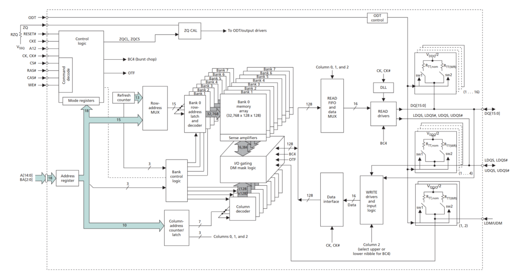
That’s 8 banks, each with 32,768 rows, and each row having 1024 columns. And because the word size is 16 bits, that’s 8 * 32,768 * 1024 * 2 = 512MB per chip. Accordingly, the AXI address will need 15 bits for row, 3 bits for bank, and 10 bits for column, and we’ll probably stick with the default row-bank-column configuration
Zynq uses a single rank, two chip setup, where each chip’s DQ width is 16 bits, and together they form a 32 bit interface. Each chip has 8 banks, each with it’s own sense amplifiers, rows, and columns. The chips are clocked at 533MHz, and since data can be transferred on both the rising and falling edge, we can get up to 1066MT. Burst size is 8, unless we use BC4 (chop) mode
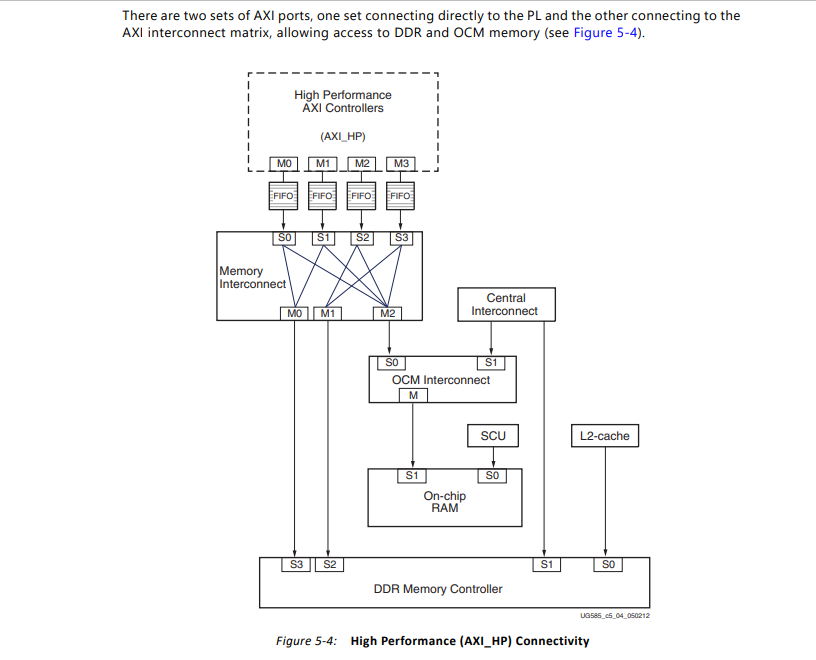
The PL side (FPGA) talks to the memory controller through four high performance AXI slaves, HP0, HP1, HP2, and HP3. The slaves have a Fmax of 250MHz, and can be configured to be 32 or 64 bits
With that said, let’s calculate a read speed of light for the DDR controller. In the best case, with no thrashing and all requests hitting an open row (and ignoring refresh), that’s 2 chips x 16 bits x 1066MT = 3.97116 GB/s, when it’s not servicing requests from higher priority clients like the L2 cache. And since the memory controller efficiency for sequential reads is 97%, let’s say 3.8520252 GB/s is the best we can hope for. OK, so what does that mean? Well, assuming all video games are legally required to ship at 16.666ms, that would be 112 passes reading from a fullscreen texture
If AXI slaves are clocked at 250MHz, and we use 64bit beats, the four slaves can transfer a combined 32 bytes per clock, about 8 GB/s, or 217 fullscreen write-only passes. Now, I can promise you that you will see no such speed. First of all, you cant just assume perfect parallelism and multiply by 4. The HP slaves have request FIFOs that fill up very fast, and at some point you’ll face DDRI arbitration. DDRI has four 64-bit AXI memory ports: one AXI for the CPU/ACP L2 cache, two that are shared by our HP slaves, and another for the other bus masters
OK, that wasn’t exactly actionable information, so now we need tests to answer the following questions:
- Is there any benefit to 64 bit AXI transfers over 32 bit ones?
- Can we saturate with only one high performance slave, or do we need to use all four?
- How far can we lower the AXI clock before it becomes the bottleneck?
- What is the shortest transfer length we can get away with before full AXI FIFOs become an issue?
- What combination of parameters result in the best performance?
- How close can we get to the DDR controllers transfer limit?
- How badly do writes affect reads, and vice versa?
- Conversely, do we need both reads and writes to saturate?
- Bonus question: how intentionally bad can we make things by row thrashing?
- I know there is a CAM, but how good is transaction reordering at hiding the latency of precharge and open
Methodology and Tests
The methodology is simple: read and/or write all 1GB (minus 512KB) of DDR, and use perf counters to count the number of cycles. Each of the four AXI masters has separate read address, read data, write address, and write data procedural always_ff blocks, and they just spam the HP slaves as fast as the requests can be accepted. The tunable parameters are number of slaves, burst length, bytes per beat, AXI clock speed, and whether reads and writes happen simultaneously. The perf counter values are then read via AXI and displayed in Vitis. The goal is not just to see what’s necessary to max out bandwidth, but also to see how reads and writes affect each other, as well as finding the minimum AXI clock we can use without it becoming the bottleneck
Note: for these tests, all transfers are set to non-cacheable and non-bufferable, so there shouldn’t be any 32 -> 64 upsizing
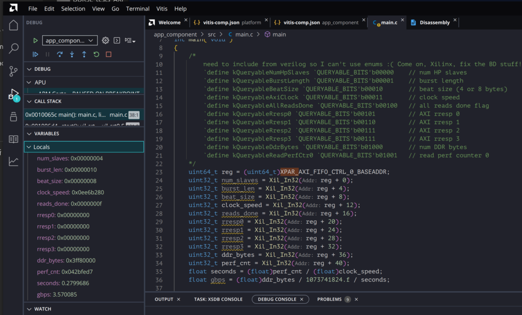
Test 0: Only reads at 250MHz
Here are the results from the first 30 tests. Green represents only one HP slave, red shows two, and blue is four. Solid lines are tests with a 4 byte beat size, and dashed lines are 8 bytes. X axis shows burst length, and Y shows GB/s
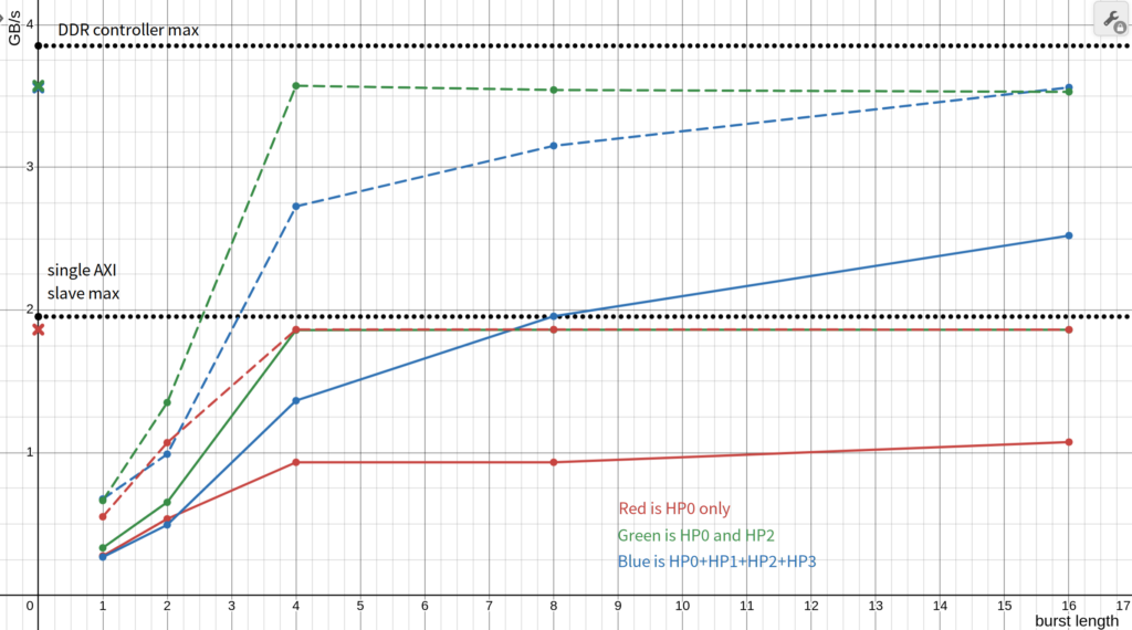
Well, that was… expected. Dashed lines are always better than solid lines, and so you always want to use the 64 bit beat size. As for burst length, I’d aim for at least 8, but optimally 16 if you can.
The single slave case gets pretty close to AXI’s max perf expected from a single HP slave. I maxed out around 1.86185 / 1.95313 = 95%, with the difference probably being mainly down to overhead.
The two slave case seems quite a bit better than the four slave case for burst lengths less than 16, which I suspect might come down to arbitration. To test this, I tried switching from using HP0+HP2 to using HP0+HP1, since they share a port, and the performance was lower. I’m not 100% convinced this explains the differences, but I might want to add perf counters to track how many clocks the AXI FIFOs are full in the future to further dig down into what is going on
So far, we’ve only managed to hit 3.560393 / 3.8520252 = 92.429% of the expected DDR controller performance, and I am curious why this is. As a fun test, I tried a very approximate calculation. OK, deep breath. My DDR chip is speed grade -125 with parameters 7-7-7, meaning the tRCD (row to column delay) is 7 cycles, and the tRP (row precharge) is also 7 cycles at the 533MHz DDR clock. So, that is
previous row precharge: tRP = 7cy × 1.876 ns = 13.132 ns
activate the new row: tRCD = 7 × 1.876 ns = 13.132 ns
total cost per row: 13.132 + 13.132 = 26.264 ns
The chip has 8 banks, each with 32,768 rows, and so each slave has to cover 65,536 rows.
65,536 rows x 26.264 ns = 1,721,238 ns total cost
1,721,238 ns / 4 ns (250MHz) = 430,310 cycles
(0x042ee70f – 430,310) / 250MHz = 0.279009444 seconds
0.99951171875 GB / 0.279009444 seconds = 3.582358 GB/s
Or 93% of the speed of light, compared to the previous result of 92.429%. Time to further embarrass myself with more suspicious calculations of dubious value. Since banks can refresh rows in parallel, the full refresh cost for the estimated four full refreshes would be 860,620 cycles of the 250MHz clock, giving an estimated 3.6271 GB/s, or 94.16% the speed of light (if we were allowed to just subtract time like that)
OK, at this point, I’m almost willing to believe that 5% loss to system inefficiencies and thermal fluctuation is plausible. I’d obviously like to do more tests to find out where the bottlenecks are, but for now I moving on instead of artificially inflating the post word count any further
Test 1: How low can your AXI clock go
Since the two and four slave tests are far below the limit for AXI, but right below DDR controller limit, it feels safe to assume we’re DDR controller bound. Let’s prove that by lowering the AXI clock to show its not the limiting factor. A good initial guess is to assume everything is perfectly efficient and parallel, and then solve C = 1,073,217,536 bytes / 8 bytes per beat / 4 slaves / 0.25947694183 seconds. We get C = 129MHz, so that should be the minimum clock speed needed to hit the target bandwidth. Now let’s see the actual observed curve!
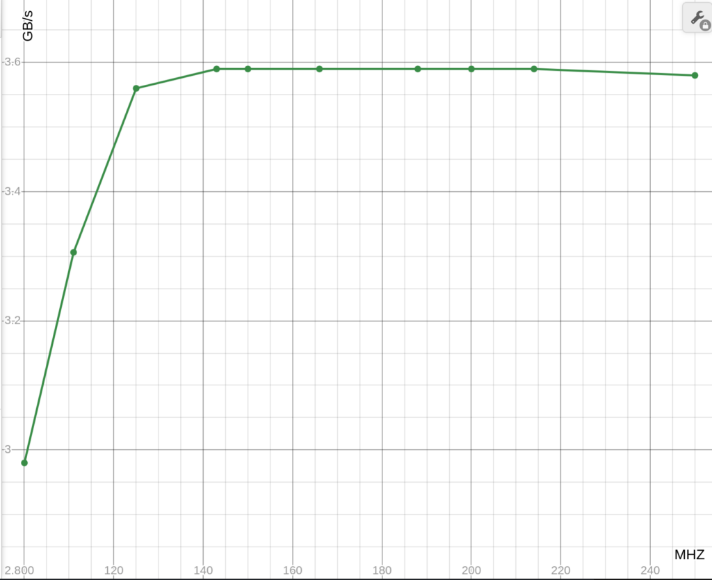
Uhhh that’s pretty close. Maybe a bit too close. So suspiciously close that I’d probably accuse me of fraud if I wasn’t me. So it looks like if you want to hit max bandwidth, you might be able to safely get away with about 140MHz or 150MHz, far below the 250MHz I’d been foolishly using up until now. Enjoy your power savings and easy timing closure
Test 2: The write stuff
GPUs don’t just read from memory, but they also… *checks notes* … write to memory from time to time as well, so it’s probably worth checking how simultaneous reads and writes affect each other. AXI can handle parallel reads and writes just fine, but we should know how the rest of the system likes it
The read part of the test remains unchanged. We’ll still be spamming reads of all of DDR as fast as the commands are accepted. Writes do the same, but this is going to introduce an issue. Any one HP slave is likely to be hitting the same bank, but different rows. In other words, we’re going to be getting some pretty bad row thrashing
What I am hoping to see is a somewhat even split of the previously achieved bandwidth without much loss, but I suspect that won’t happen. Factoring in a wild guess penalty of 10%, and assuming we’re still DDR controller bound and not AXI bound, I’m going to take an initial guess of 3.56 * 0.9 (penalty) / 2 (read and write), which gives a nice round 1.6 GB/s
So, what are the results? 1.49 GB/s write and 1.43GB/s read. Ouch! Even if every row of every access missed, unlikely as that might be, that would be around a 0.0054096 second increase in time, so I’m not suspecting that’s the main culprit. However, since there’s like zero chance I’ll be able to sleep tonight until I can know the effect row thrashing had on the numbers, I am going to run the actual experiment
This time around, instead of each slave both reading and writing it’s two banks, it’s going to read all of bank A and write all of bank B to ensure no thrashing. With this configuration, read bandwidth moves up to 2.52 GB/s and write bandwidth is increased to 2.600 GB/s. So yeah, row thrashing did have a noticeable effect, but it seems the main inefficiencies are elsewhere in the system
I’m also kinda interested why the write numbers are so much better despite write efficiency being worse than read inefficiency in the DDR controller. I can’t prove any of this yet, but I have a few ideas. First, the perf counter increments until the final bresp arrives, but that could be far before the writes actually commit. Next, there seems to be aggressive buffering, reordering, and write combining of writes. Finally while I didn’t see any mention of an explicit write bias in the DDR controller, it might be a secondary effect of the bias towards same type and same page accesses
Conclusion
Yeah, I dunno, disappointment is a part of life, and you go to war with the memory system you have, not the memory system you want. I guess I have alot of creative latency hiding and cache efficiency improvements in my future, so at least that’s something fun to look forward to!
This was a pretty shallow look at things, focusing more on measurements and less on the reasons why things are what they are. That means that in the likely case I misunderstood something, or missed some important setup, I might be able to get back some of the performance lost to my old friend “inefficiencies”. I do plan on doing more of a deep dive in the future so occasionally check this blog post for updates
Important references
Zybo Reference Manual
Zynq TRM
Datasheet for my chip
Address Mapping
