一所懸命HWデザイナーのふりをやっとる現代のC++が大嫌いなSWの開発者。FPGAのGPUとレトロな家庭用ゲーム機を作ること、うちの猫(ニュートリノ+コスモス)、お箏の演奏、ゲーム開発、抹茶+和菓子がめっさ好きやねん。tweetsは私個人の意見で、会社を代表するものやない
In the last post, I combined a setup tutorial with creating a fun and useful bit of our GPU: HDMI. I will be trying the same thing here, but unlike last time, it’s not going to be fun. I mean command buffers are obviously fun, but working with Vitis for Zynq can be challenging. If you are using Zynq and want to follow along, now is a good time to make sure you downloaded the latest Vitis as mentioned in my first post. You’re also going to want to get comfortable with AXI since that seems to be what most of the Zynq universe runs on. It may seem daunting at first but the protocol itself isn’t that hard, and you’re only going to need to support an absolute minimal subset
Part 0: Command Buffer Medium Dive
Command buffers are one of the main ways the CPU will talk to our GPU. We’ll be adding commands for drawing triangles, reading and writing GPU registers, writing and conditionally waiting on labels, NOPs, and some branching like jump/call and return. All commands are 64 bits, with the exception of NOPs which are used to allocate space in the command buffer in 64 bit units for inline data. Here are some of examples of what commands can look like
// write MMIO GPU reg: 4 bits header + 2 bits reg aperture + 3 bits reg offs + 32 bits payload
typedef struct packed
{
	// upper 32 bits
	FrontEndPacketOpcode opcode;
	GpuRegsMmioAddr mmio_reg_addr;
	logic [32-$bits(opcode)-$bits(mmio_reg_addr)-1:0] reserved_hi;
	// lower 32 bits
	logic [31:0] payload;
}
FrontEndPacketMmioWrite;

typedef enum bit [0:0]
{
	kLabelWriteEventAlways,
	kLabelWriteEventGfxDone
}
LabelWriteEvent;

// all memory packets use the same layout to simplify decode
// very important that this lines up for jumps, label ops, and NOPs
`define FrontEndAddressPacketHiWord(flagname)		\
	FrontEndPacketOpcode opcode;			\
	logic flagname;					\
	FrontEndLabelAddr address

// write memory label: 4 bits header + 1 bit event + 27 bits addr + 32 bit write val
typedef struct packed
{
	// upper 32 bits
	`FrontEndAddressPacketHiWord(write_event);
	// lower 32 bits
	logic [31:0] payload;
}
FrontEndPacketLabelWrite;

// placeholder until I think that would be most useful
typedef enum bit [0:0]
{
	kLabelWaitCmpFuncEq,
	kLabelWaitCmpFuncReserved
}
LabelWaitCmpFunc;

// wait memory label: 4 bits header, 1 bit cmp func, 27 bits addr, 32 bit refval
typedef struct packed
{
	// upper 32 bits
	`FrontEndAddressPacketHiWord(cmp_func);
	// lower 32 bits
	logic [31:0] refval;
}
FrontEndPacketLabelWait;
Label writes can happen either immediately or when previous work finishes. Label waits can (in theory) support two compare functions, but currently only EQ is supported. Jumps need to support a range of cases, such as looping, jumping to another command buffer, and call/return with a few restrictions coming from needing to know the callee’s size ahead of time. So for example if command buffer A calls B, the size of B must be known at that time, so no more commands can be added to B after the return. This is mainly to help meet timing and reduce address muxing.
Our story begins when the CPU writes the command buffer start address to an MMIO register, and the end address to another. That second write magically adds the submit to a FIFO, where it can eventually be consumed by the front end state machine. There is a third MMIO status reg that can be read from the CPU to query if its safe to submit another command buffer
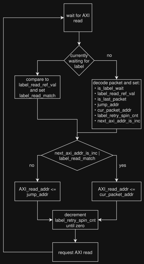
When the front end FSM sees a non-empty FIFO, it transitions from idle to update, and calculates the AXI read address. The first time around, this will be the address of the first command, but subsequently can be the address of the next command, a jump address, or the address of a label to query. It then moves to the fetch state where it waits for the data to arrive. Once the data arrives, its either decoded as a command, or if we’re currently waiting on a label, the data is compared to the reference value to see if it matches. It then moves back to the update state and continues until the last command.
The AXI read address calculated in the update state is
// getting a little involved. In normal cases opcode[3:2] means the AXI address field is the next packet address, but if the
// previous read was label data, the opcode can't be trusted. But if the label in memory matches the reference value,
// then the next AXI read should be the next packet
AXI_read_addr <= (next_axi_addr_is_packet_incr | label_read_match) ? cur_packet_addr : jump_addr;
Here, jump_addr holds the jump target encoded in the current command. If the command is really a jump, this becomes the next fetch address. The brilliantly* named cur_packet_address holds the… wait for it… next packet address, as in current_addr + 1. In the case of a non-jump command or a wait label match, this is the address we want to fetch the next command from
But what about wait labels that don’t yet match? In that case, both next_axi_addr_is_packet_incr and label_read_match will be false, meaning we use jump_addr of the last fetched command. Luckily the label wait command’s address field lines up perfectly with the address field of the jump command, and so using the jump address results in AXI reloading the value from the label address (after a programmable-length retry spin)

Small performance note: you’ll notice there is currently no command prefetching or pipelining. Sure, that’s not great, but I’m just not convinced burning area on the prefetch and invalidate logic is going to be a massive win here. Actually, there is another reason I didn’t want to do prefetching: label writes can also be used to write to the command buffer itself! Label write addresses are 64b aligned, but they only write 32b, so if the parts of a packet we want to overwrite happen to occur in the LSB32, we can change them from a write label command. Example: both the draw triangle’s vertex offset and vertex count, and the MMIO write’s payload occur in the LSB32, and therefore can be overwritten by label write
Part 1: A Basic MMIO System
OK, with the fun part over, it’s time to get this working on Zynq. Because command buffers are submitted via MMIO writes, we need a way to do this. There are three parts to the rest of this post: 0) getting used to the Block Design tool by implementing basic DDR reads and writes, 1) implementing a basic MMIO register system, and 2) doing the software SDK-side work in Vitis. Using Zynq requires some very simple AXI functionality, so hopefully you watched the short videos above, and are comfortable with the secret handshake
Let’s start with getting used to the Block Design tool by doing some DDR writes and reads. Create a project for your Zynq board like we did in the last post, but this time instead of creating a SystemVerilog top level module, be sure to create a Verilog one. Why would we do such a thing in the year of our lord 74? Well, the Vivado block design tools still don’t recognise or parse SystemVerilog files, so we need to create a Verilog file to instantiate the SystemVerilog top level module inside of
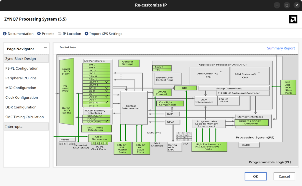
Under Flow Manager → IP INTEGRATOR, click on Generate Block Design, click the + button to add IP, and select Zynq7 Processing System. There should be a green banner at the top of the screen that says Run Block Automation that you’ll want to click to customise the IP for your board. Once that finishes, you can double click on the Zynq block and have a quick look around. On the right will be a connectivity diagram showing how the CPU and FPGA work together, and on the left will be a list of customisable things. You may not understand everything in there, but with sections such as DMA, fabric interrupts, and clock configuration, your heart is probably racing thinking about all the possibilities and cool stuff you can do

We can play with all that fun stuff another day, but right now we only need to change two things. First we need to enable a fabric clock. This will be used as both the AXI bus clock, and our main GPU clock, allowing me put off having that CDC talk until another day. We also need to enable one of the high performance AXI slaves, as AXI is how the FPGA programmable logic side interfaces with DDR
So go ahead and enable FCLK_CLK0 under Clock Configuration → PL Fabric Clocks, and set it to *some* number of MHz. I usually try to target 200MHz and above, but for this test, anything reasonable is OK. Next you’ll want to enable S_AXI_HP0 Interface under PS-PL configuration → HP Slave AXI Interface. Finally, add a clock input port and your AXI ports to your Verilog top level module
`timescale 1ns / 1ps
`default_nettype none

// all my wrapper macros for declaring and connection AXI ports
`include "axi_params.vh"

module verilog_top(
	input wire /*logic*/ gfx_clk,
	// macro so I don't have to manually declare ports
	`DECL_HP_AXI3_VERILOG_PORTS(0));

	// instantiate the SV module inside the verilog one
	gpu_top sv_top(
		.gfx_clk(gfx_clk),
		// macro so I don't have to manually connect everything
		`CONNECT_HP_AXI_PORTS(0));
endmodule
Back in the Diagram pane, right click on some empty area, choose Add Module, and select your Verilog module from the list. An option to run Connection Automation should appear, but it’s probably more educational to do it yourself
First, connect the Zynq’s FCLK_CLK0 pin to your Verilog module’s gfx_clk, and also to the Zynq’s M_AXI_GP0_ACLK and S_AXI_HP0_ACLK. This takes the fabric clock and connects it to all the things that want to use it
If you defined your S_AXI_HP0_0 ports in a way that matches what Vivado expects, Vivado can usually deduce that your module is an AXI interface, and allow you to directly connect it to the Zynq’s S_AXI_HP0. Again, this only works if your AXI signals are all the exact right number of bits. One bit off, and Vivado may not recognise it as AXI, and not allow you to connect it. With all that done, your connected diagram should look like this

However if you validate the design (F6 button), you will probably get the following error

To fix it, we need to tell Vivado the actual clock speed for our AXI interface. Click on S_AXI_HP0_0 in your module, then go to Block Interface Properties → Properties → CONFIG → FREQ_HZ and set it to your FCLK_CLK0 frequency. You should now be able to successfully validate your design. Before moving on, why not take a few seconds to look at the Address Editor as well. Right now we only have one AXI thing, but as we add more, that is how we’ll assign address ranges to each device
There is one final thing to do before we can synthesize the design. Under sources, find design_1 (design_1.bd), right click it, and choose Create HDL wrapper. Let Vivado manage it (for now). When that is done, go back to the Sources tab, right click on design_1_wrapper (design_1_wrapper.v), and choose Set As Top, making the generated design wrapper the new top level module. There are some times you may want to keep your RTL module as top, and instantiate the Zynq inside it, but not today
You can now run synthesis, implementation, and bitstream generation, but you should probably write some actual RTL to make your design do something first. I suggest a very simple AXI master state machine to test FPGA writes to memory by reading the expected values back afterwords, and lighting up an LED if there is an error. Its a simple way to make sure you can communicate with DDR via AXI and verify everything is connected and working
Pro tip: I should also mention that if you change your RTL source, especially SystemVerilog files, it’s possible Vivado won’t see the changes, and synthesize old code. To really make sure Vivado sees changes, you always need three steps: click on the Refresh Module References banner in the Diagram view, right click on design_1.bd in the sources view and select Reset Output Products, and then select Generate Output Products. There is also a bug I helped Xilinx track down where the Refresh Module References banner doesn’t show up, but I am told it will be fixed in the next version?
Let’s implement the MMIO system, so we can control the front end from the CPU and send command buffers. In the previous section, we created a AXI master that connected to high performance slave S_AXI_HP0. That is because the FPGA fabric is the thing to initiate transfers. This time we will be making an AXI slave, and connecting it to the AXI master m_AXI_GP0 so that the CPU can control things with writes to our chosen memory range
`timescale 1ns / 1ps
`default_nettype none

`include "axi_params.vh"

module mmio_reg_slave(
	input wire /*logic*/ gpu_clk,
	`DECL_AXI3_WIDTH12_SLAVE_PORTS,
	// send the received data to anyone who cares
	output wire /*logic*/ valid_out,
	output wire /*logic*/ [31:0] addr_or_data_out);

	// AXI slave, recieve address and put it on the bus
	// then recieve data and put it on the bus
	// some of these write to regs backed by actual storage
	// others just decode to signals that do *things*
Just like the previous example, you need to add the mmio_reg_slave module in the Block Design tool, connect gpu_clk to the fabric clock, and connect the S_AXI slave port to Zynq’s M_AXI_GP0 port. After adding the bus and valid ports to verilog_top_0, we can then also connect valid_out and addr_or_data_out. The idea is that The CPU writes data to a specific address range, the slave recieves the address and data, and then forwards it to our Verilog top module ports mmio_valid_in and mmio_addr_or_data_in where it will eventually be used to add command buffers to the front end FIFO

I mentioned that the CPU can submit command buffers by writing to a specific memory range, but I didn’t say what that range is. Please turn your attention back to the Address Editor you saw previously. Before we only had one network for HP0, so it wasn’t that interesting, but now a second network has appeared, and we need to assign it a base address and size

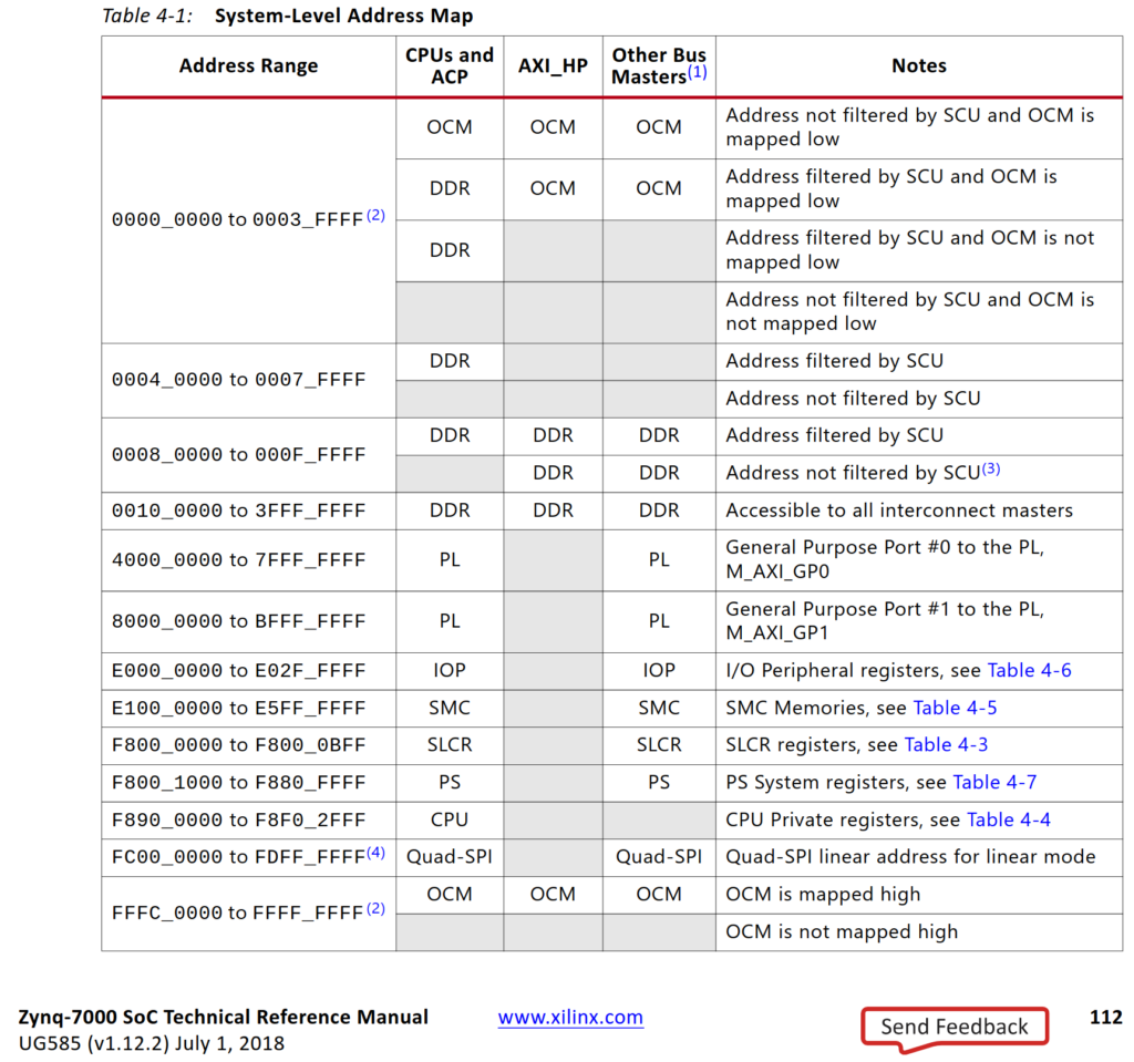
So it looks like 4000_0000 is a good start address for our MMIO register writes, since we’re using M_AXI_GP0. Let’s reserve the first 4KB for the slave we made, and if we add another slave, it can use the next 4K area up. Sadly 4K is the minimum selectable area
There are two DDR ranges: 32’h80000 to 32’hFFFFF (524,287 bytes), and 32’h100000 to 32’h3FFFFFFF (about a gigabyte). We’ll be using 0 to 32’h3FFFFFFF to allow accessing all of DDR plus OCM, and so the new address assignments becomes

Part 2: Making The Software SDK in Vitis (cliffhanger!)
This brings us to the final part of the tutorial. You finished coding the front end state machine, you made your AXI master for reading from DDR, and you made your AXI slave for recieving command buffer submissions from the CPU. Or maybe you’re taking it slow and just made a thing to toggle LEDs via register writes from the CPU? Either way, it’s time to do the CPU SDK side in Vitis. However, since this post is already too long, I will save the Vitis tutorial for the next post